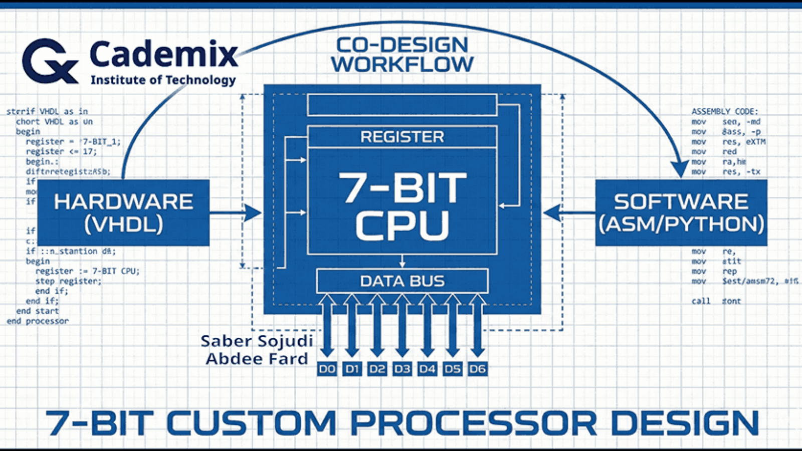
I built a compact 7-bit processor to explore hardware–software co-design end-to-end: defining a minimal instruction set, implementing the datapath and control in VHDL, and closing the loop with a small assembler that produces ROM-ready binaries. The design focuses on a small core of operations LOAD, ADD, SUB, and JNZ with an extended MULTIPLY instruction implemented using a shift-and-add approach to keep the hardware simple. Internally, the processor is decomposed into familiar blocks (ALU, register file, program counter, instruction register, ROM, and multiplexers), with a control unit described as an ASM-style state machine that sequences fetch, decode, and execute. A four-register file (R0–R3) and a zero flag provide the minimum state and condition mechanism needed for basic control flow. To integrate software with the hardware model, I use a Python-based assembler that converts assembly-like inputs into the binary encodings expected by ROM initialization. The project is intended to be validated in simulation by observing program counter progression, register updates, and ALU outputs under representative instruction sequences.
Saber Sojudi Abdee Fard
Introduction
I designed this project to practice hardware–software co-design in a setting small enough to reason about completely. The core idea is straightforward: define a minimal instruction set, implement a complete processor around that ISA in VHDL, and connect it to a simple software tool a Python assembler that produces the exact 7-bit encodings the hardware expects. The result is an offline simulation workflow where I can iterate on both sides of the boundary: instruction semantics in hardware and program encoding in software.
The processor is intentionally constrained. Both data and instruction representations are 7 bits wide, and the ISA is limited to a small set of operations: LOAD, ADD, SUB, JNZ, and an extended MULTIPLY. Memory is ROM-based, and the goal is correctness and clarity in simulation rather than breadth of CPU features or performance. Within that scope, the design targets a complete “compile -> encode -> load -> simulate -> inspect” loop: compiling and simulating the VHDL modules, translating an assembly-like program through Conversion.py, loading the produced binary into Memory.vhd, and then validating behavior by inspecting the program counter, register updates, and ALU outputs in the simulator.
This article explains the system the way I worked with it: as a set of contracts between modules and between software and hardware. I focus on the architectural decomposition (datapath and control), the encoding boundary enforced by the assembler, and what constitutes a successful run in simulation. I also call out the explicit non-goals such as advanced control-flow features, richer memory models, or microarchitectural optimizations because the constraints are part of what makes the design teachable.
Methodology
Architecture overview
I implemented the processor as a small set of composable VHDL building blocks connected around a single 7-bit internal bus. The top-level entity (Processor) exposes CLK and RESET inputs and exports the four general-purpose register values (R0out–R3out) specifically to make simulation inspection straightforward.
Inside Processor.vhd, the datapath is wired as follows:
- A ROM (
Memory) outputs a 7-bit word (MData) addressed by the program counter output (PC_OUT). - Two 4-to-1 multiplexers (
MUX4x1) select ALU operands from the four register outputs (ROUT0–ROUT3). Each mux is driven by a 2-bit selector (S0for operand A,S1for operand B). - The ALU computes a 7-bit result (
ALURes) based on a 2-bit command (CMD). - A 2-to-1 “bus mux” (
MUX2x1) selects what drives the shared internal bus (BUSout): either ROM data (MData) or the ALU result (ALURes), controlled byBUS_Sel. - The shared bus is then assigned to a single internal input (
RIN <= BUSout) that feeds every state-holding element: the four registers, the instruction register (IR), and the program counter (PC) load their next value fromRINwhen their respective load control is asserted.
This wiring creates a clean contract boundary: computation happens in the ALU, storage happens in registers/IR/PC, and the only way values move is by selecting a source onto the bus and latching it into a destination on the next clock edge.
A control unit (control_unit) sits beside the datapath. It consumes the current instruction (ROUTIR, the instruction register output) and per-register zero indicators (ZR0–ZR3), and it drives all load/select signals: LD0–LD3, LDIR, LDPC, INC, BUS_Sel, plus the ALU command (CMD) and the two operand selectors (Sel0, Sel1).
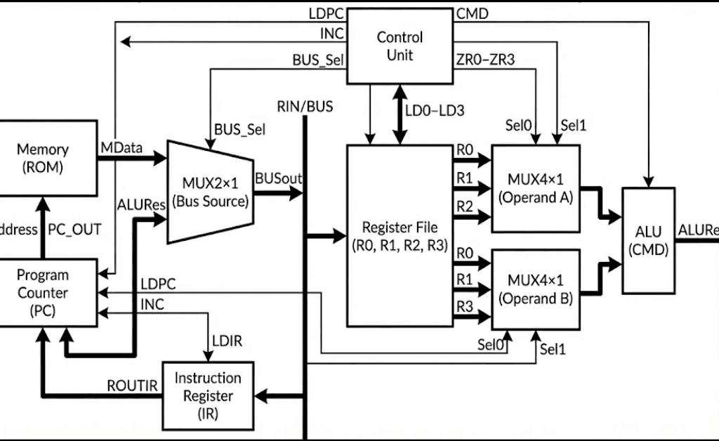
Figure 1 — The ROM, register file, and ALU are connected through a single bus-source mux that drives a shared internal bus (RIN), while the control unit sequences selects and load-enables for fetch and execute.
Control unit and instruction sequencing
I implemented the controller as an explicit enumerated-state machine in control_unit.vhd. The control unit decodes two fields from the 7-bit instruction:
y <= ROUTIR(6 downto 4)as a 3-bit opcode.x <= ROUTIR(3 downto 2)as a 2-bit register selector (converted to an integerReg_numfor indexing the zero-flag vector).
The control flow uses these states (as defined in the state type): S0, S1, D, S2, S3, S4, S5, S6, S7, and S8. Operationally, they map to a compact fetch–decode–execute loop:
- Fetch (
S0): the controller assertsLDIR <= 1while selecting ROM data onto the bus (BUS_Sel <= 0). In the same state it assertsINC <= 1to advance the PC. Conceptually, this state is responsible for “IR <- M[PC]” and “PC <- PC + 1”. - Stabilize (
S1): the controller deassertsINCandLDIRand transitions to decode. - Decode (
D): the controller either halts, dispatches to an execute state based ony, or evaluates a conditional branch using the selected register’s zero flag.- A literal all-ones instruction (
ROUTIR = "1111111") is treated as halt and transitions intoS2, which self-loops. - If
y = "000", it dispatches to Load (S3). - If
y = "001", it dispatches to Add (S4). - If
y = "010", it dispatches to Sub (S5). - If
y = "100", it dispatches to Multiply (S8). - Otherwise, it treats the instruction as a conditional PC control operation that consults
ZR(Reg_num)and chooses betweenS6(load the PC) andS7(skip).
- A literal all-ones instruction (
The execute states drive the datapath in a very direct way:
- Load (
S3) asserts exactly one ofLD0–LD3based onx, keeps the bus sourcing from ROM (BUS_Sel <= 0), and assertsINC <= 1before returning to fetch. This matches a “load immediate/data word from ROM and step past it” pattern. - Add/Sub/Multiply (
S4,S5,S8) select registers into the two ALU operand muxes (Sel0,Sel1), setCMDto the operation code ("00"for add,"01"for sub,"10"for multiply), switch the bus to the ALU result (BUS_Sel <= 1), and assert one ofLD0–LD3to latch the result back into a register. In the current implementation, both operand selectors are derived from the same instruction field (xandROUTIR(3 downto 2)), so bothSel0andSel1are driven from the same two-bit slice. - PC load (
S6) assertsLDPC <= 1while selecting ROM data onto the bus (BUS_Sel <= 0) and returns to fetch. In combination with the top-level wiring (ROM addressed byPC_OUT, bus sourcing fromMData), this implements an indirect jump target read: the PC loads the 7-bit word currently stored at the ROM address. - PC skip (
S7) assertsINC <= 1and returns to fetch. This acts as the complementary behavior toS6: when the condition is not met, the controller advances past the jump operand word.
That last pair (S6/S7) is a key contract in the design: conditional control flow is implemented by placing a jump target word in ROM immediately after the branch instruction, then either loading the PC from that word (taken) or incrementing past it (not taken). This keeps the instruction format small while still enabling label-based control flow at the assembly level.
Datapath components and local contracts
I structured the datapath around a small number of synchronous state-holding elements (registers, program counter, instruction register) and purely combinational plumbing (multiplexers and the ALU). The shared internal bus (RIN) is the only write-back path: every storage element loads from the same 7-bit value when its load-enable is asserted. That design choice keeps the movement of data explicit each cycle is “pick a source onto the bus, then latch it into one destination” which makes it straightforward to debug in simulation.
Register file and zero flags (Reg.vhd)
Each general-purpose register is implemented as a simple rising-edge latch with a load enable. The register stores a 7-bit vector (res) and continuously computes a per-register zero flag ZR. In this implementation, ZR is asserted high when the register content is exactly 0000000, and deasserted otherwise. Because the zero flag is derived from the stored register value (not the ALU result), conditional control flow is defined in terms of “what is currently in the selected register,” which is a clean contract for a small ISA.
A practical implication of this choice is that the condition mechanism is transparent to inspection: in simulation, I can interpret the branch condition by looking at the register value and its corresponding ZR* signal without needing an additional flag register.
Program counter semantics (PC.vhd)
The program counter is another 7-bit state element with three control inputs: CLR (asynchronous clear), LD (load from the bus), and INC (increment). The implementation uses a single internal accumulator (“inBUS” inside the clocked process) that can be loaded and incremented in the same cycle. If both LD and INC are asserted on a rising clock edge, the update order is “load, then increment,” which gives a well-defined behavior for any state machine that wants “PC <- operand + 1” rather than forcing two cycles.
In the top-level wiring, CLR is driven from the processor’s reset line (mapped through the RST signal), and the fetch phase relies on INC to advance sequentially through ROM addresses.
Instruction register (IR.vhd)
The instruction register is a minimal latch: on a rising clock edge, if LD is high, it captures the current bus value into an internal signal and exposes it as ROUT. There is no decode logic here by design; the controller consumes the raw 7-bit instruction word. This separation keeps “instruction storage” distinct from “instruction interpretation,” which is useful when iterating on encodings during co-design.
Combinational multiplexers (MUX2x1.vhd, MUX4x1.vhd)
I used two mux types:
- A 2-to-1 mux selects the shared-bus source. In the current design,
S=0selects ROM data andS=1selects the ALU result. This switch is effectively the “read vs compute” gate for the entire machine. - A 4-to-1 mux selects ALU operands from the four register outputs. The selector is two bits wide, built by concatenating the select lines inside the mux and mapping
"00","01","10","11"toR0,R1,R2,R3.
Both muxes are purely combinational. That means the timing contract is simple: control signals must be stable in time for the selected value to propagate to the bus (or ALU inputs) before the next rising edge, where it can be latched by the destination element.
ALU behavior and truncation (ALU.vhd)
The ALU accepts two 7-bit operands and a 2-bit CMD:
"00"performs unsigned addition."01"performs unsigned subtraction."10"performs multiplication via a shift-and-add loop.
Internally, both inputs are resized to 14 bits to allow intermediate growth during addition/subtraction/multiplication, and the multiplication iterates over the bits of IN1: for each set bit IN1(i), the ALU adds IN2 shifted left by i into an accumulator. This is a direct, minimal-hardware way to express multiplication in behavioral VHDL.
The key architectural contract is at the output: the ALU always returns only the lower 7 bits of the 14-bit intermediate result. In other words, arithmetic is effectively performed modulo (2^7) at the architectural boundary. That choice is consistent with the project’s 7-bit scope, but it also means overflow is handled by truncation rather than saturation or flagging.
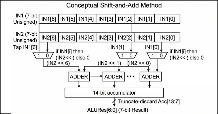
Figure 2 — Conceptual shift-and-add multiplication accumulates (IN2 << i) for each set bit IN1[i] into a 14-bit sum, then returns only the lower 7 bits as ALURes[6:0].
ROM and “program as VHDL” workflow (Memory.vhd)
The memory is implemented as a 128-entry ROM (instruction(127 downto 0)), addressed by the 7-bit program counter. The output is a direct combinational lookup: Data <= instruction(to_integer(unsigned(address))). The ROM contents are currently defined by assigning specific indices inside the VHDL architecture. This matches your intended workflow: use the Python assembler to generate 7-bit binary instruction words and then paste those encodings into Memory.vhd to run them in simulation.
The file also includes multiple annotated program variants. One example sequence is commented as an “add 7 with 4” demonstration, and another is structured as a small loop intended to exercise conditional branching and repeated arithmetic. A third variant (commented out) is positioned as a “hardware focus” multiplication path, contrasting with the loop-based approach. From an engineering perspective, keeping these snippets inline makes the simulation loop fast, but it also means “program loading” is manual and tightly coupled to the ROM source code rather than being a separate artifact (e.g., a memory initialization file).
Figure placement: A code figure that shows a short ROM snippet (a few consecutive instruction(i) <= "......."; lines) is useful here to make the “assembler output -> ROM initialization” boundary concrete.
Assembler and the hardware–software boundary
To make the processor usable as a co-design exercise rather than a pure hardware artifact, I included a small Python assembler (Assembler/Conversion.py) that translates assembly-like lines into binary strings that can be loaded into the ROM. The intent, as documented in the repository, is to run the conversion step first, then paste the produced encodings into Memory.vhd, and finally validate behavior in simulation by inspecting the program counter, register values, and ALU outputs.
The current assembler implementation is deliberately minimal: it tokenizes each line by removing commas and splitting on whitespace, looks up an opcode mnemonic in a small table, and then encodes operands by type. Register operands (R0–R3) are encoded as 2-bit binary values, while any non-register operand is encoded as a 4-bit binary value. Each instruction line is therefore built by concatenating a fixed-width opcode field with one or more fixed-width operand fields, producing a binary string per line.
This assembler is also where the most important integration contract lives: the binary it emits must match the instruction word format the VHDL control unit expects. The README states the processor operates on 7-bit-wide instructions and provides an example encoding (ADD R1, R2 -> 0100010). In the current Conversion.py, however, the opcode table is 2 bits wide and only covers Load, ADD, SUB, and JNZ, with no explicit MULTIPLY support. In practice, that means the assembler represents the intended direction (software producing ROM-ready bits), but the exact bit-level encoding contract is something the project has to pin down consistently between README, assembler, and the VHDL decode logic. That “tight loop” of adjusting encodings until the fetch/decode/execute behavior matches expectations is part of the educational value of the co-design workflow.
Two targeted questions so I can describe the integration contract precisely in Section 6 (Results) and avoid guessing:
Key implementation notes
- Source grounding: the narrative is based on
README.mdand the project snapshot you provided. - Entry points: hardware at
src/Processor.vhd(top-level integration); software atAssembler/Conversion.py(assembly-to-binary conversion). - Core modules:
src/ALU.vhd,src/control_unit.vhd,src/Memory.vhd,src/PC.vhd,src/IR.vhd,src/Reg.vhd,src/MUX2x1.vhd,src/MUX4x1.vhd. - Top-level integration:
src/Processor.vhdinstantiates and wiresReg,PC,IR,ALU,MUX4x1(twice),MUX2x1,Memory, andcontrol_unit, with a single internal bus (RIN <= BUSout) feeding all loadable elements. - Control surface:
src/control_unit.vhdoutputsLD0..LD3,LDIR,LDPC,INC,BUS_Sel, plusCMD,Sel0, andSel1, and consumesROUTIRand the per-register zero signalsZR0..ZR3. - Halt sentinel: the controller treats
1111111as a dedicated halt instruction and transitions into a terminal self-loop state. - Reg.vhd: rising-edge storage with
LD;ZR=1iff the stored 7-bit value is0000000. - PC.vhd: 7-bit counter with
CLR(async clear),LD(load from bus), andINC(increment); supports “load then increment” if both asserted. - IR.vhd: rising-edge instruction latch controlled by
LD. - MUX2x1.vhd: bus-source selector between ROM (
I0) and ALU (I1) with a single select bit. - MUX4x1.vhd: operand selector over
R0–R3driven by two select bits. - ALU.vhd: unsigned add/sub; multiply implemented via shift-and-add; output is truncated to the low 7 bits.
- Memory.vhd: 128×7 ROM as an internal array with explicit per-address assignments; output is a combinational lookup addressed by
PC. - Assembler entry point:
assemble(assembly_code)consumes a multi-line string and returns a list of binary strings, one per parsed instruction line. - Assembler tokenization: commas are stripped (
line.replace(",", "")), then tokens are split on whitespace; empty lines are ignored. - Assembler encoding: registers (
R*) become 2-bit fields; non-register operands become 4-bit fields; the opcode is taken fromopcode_table. - Assembler opcode coverage:
Load,ADD,SUB,JNZare defined; other instructions (includingMULTIPLY) are not represented in the table. - Hardware inspection points:
ProcessorexportsR0out–R3outexplicitly, which makes it practical to validate instruction effects without adding extra debug modules. - Software-to-hardware boundary:
assemble(...)emits binary strings from assembly-like lines; in the validated workflow these are used to populate the ROM inMemory.vhd. - Intended ISA surface: the README presents
LOAD/ADD/SUB/JNZplus an extendedMULTIPLY, and frames validation as monitoring ALU output, register values, and program counter progression during simulation. - Documentation positioning: the README positions the project explicitly as a simulation-driven, educational processor build with a minimal ISA and a Python conversion step.
- Encoding contract hotspot: the assembler’s opcode table and
assemble(...)are the natural enforcement point for a single instruction-format contract once the bit layout is finalized.
Results
Because I did not build a dedicated VHDL testbench, validation for this project is based on interactive simulation: compiling the full design, loading a short program into the ROM, and then stepping the clock while inspecting the program counter, instruction register, control signals, ALU result, and the four register outputs. This approach matches the project’s educational scope: the primary outcome is a working hardware–software loop where I can translate assembly into binary, paste those encodings into the ROM, and observe the machine executing fetch–decode–execute in a waveform viewer.
Validation checkpoints
In practice, “success” in simulation is visible as a small set of repeatable checkpoints:
- Fetch discipline: on each instruction boundary, the instruction register captures the ROM output while the program counter advances, yielding a stable next instruction word and a monotonic PC sequence.
- Load path correctness: a
LOADsequence routes ROM data onto the internal bus and latches it into the selected register, so the register output changes exactly on the intended clock edge. - ALU path correctness:
ADDandSUBroute the ALU result onto the bus and latch it back into a register; the ALU output changes combinationally with operand selection, while architectural state changes only on clock edges. - Multiply behavior: the
MULTIPLYoperation produces a deterministic product consistent with a shift-and-add implementation, with the architectural output constrained to 7 bits (i.e., truncation on overflow) as part of the 7-bit design scope. - Conditional control flow observability: conditional branching is validated by correlating (a) the selected register value, (b) its zero flag, and (c) whether the PC is loaded from ROM or advanced past the next word. This makes the branch mechanism debuggable even without a testbench, because the condition and the control effect are both visible.
Artifacts produced
The durable artifacts from a run are simple but useful: (1) binary instruction words produced by the Python assembler and (2) waveform traces in the simulator that show the PC/IR/control/ALU/register timeline for a program. The repository also contains simulator-side artifacts (e.g., waveform databases) under src/, which is consistent with an interactive debug workflow rather than a scripted regression setup.
Discussion
This project’s strongest property is that it forces a clean interface between hardware intent and software representation. The processor design is small enough that I can reason about every signal transition, but complete enough to exercise real co-design constraints: instruction encoding decisions affect decode logic; decode logic constrains what the assembler must emit; and the ROM loading workflow becomes part of the “system contract,” not a separate afterthought.
That said, the absence of a testbench is a real limitation. Interactive waveform inspection is effective for bring-up and learning, but it does not scale to repeatable regression. Without an automated test harness, it is easy to introduce subtle contract drift for example, changes in instruction bit layout, operand field meaning, or zero-flag conventions without immediately noticing. The README asserts that the assembler “supports all implemented instructions,” but the current Conversion.py opcode table only enumerates Load, ADD, SUB, and JNZ, and it encodes operands into fixed 2-bit (register) and 4-bit (immediate) fields, which may or may not match the 7-bit instruction format you ultimately used in ROM. In a co-design project, this kind of mismatch is common and also instructive but it is worth surfacing as a deliberate boundary to tighten.
The architectural constraints are also doing real work here. The 7-bit width means arithmetic overflow is not an edge case; it is a normal mode of operation, and truncation becomes the implicit overflow policy. The ROM-based memory model similarly compresses the problem: by treating “program and data” as a static table, I avoid a full load/store subsystem and can focus on sequencing and datapath correctness. The cost is that the system is simulation-oriented, and “loading a program” is effectively editing VHDL. For the stated educational goal, that trade-off is reasonable, but it is the first thing I would change if I wanted this design to behave more like a reusable platform.
What I would tighten next
If I were evolving this beyond a learning artifact, I would prioritize three reliability-oriented improvements:
- Lock the instruction contract: define a single authoritative bit layout (fields, widths, and operand meaning) and make the VHDL decode and the Python assembler share it (even if only by generating a common table/module).
- Add a minimal self-checking testbench: one or two short programs with assertions on PC/register end state would turn interactive validation into repeatable regression.
- Separate program data from RTL: move ROM initialization into a file-based mechanism supported by the simulator (or at least generate
Memory.vhdprogram blocks automatically from the assembler output) to reduce manual copy/paste drift.
Conclusion
I built this 7-bit processor as a compact hardware–software co-design exercise: a minimal ISA, a VHDL implementation with a clear separation between datapath and control, and a Python assembler that translates human-readable instructions into ROM-ready binary. The design is intentionally constrained 7-bit width, ROM-based memory, and a small instruction set so that the full fetch–decode–execute behavior remains understandable in simulation. Within that scope, the project demonstrates the engineering mechanics that matter in larger systems: defining module contracts, sequencing state updates cleanly, and keeping the software encoding pipeline consistent with hardware decode expectations.
The next step, if I want to make it more robust, is not to add features first; it is to formalize the instruction-format contract and add a minimal self-checking testbench so that the co-design boundary becomes repeatable and verifiable rather than primarily manual.